PCB Manufacturing and Assembly: Everything You Need
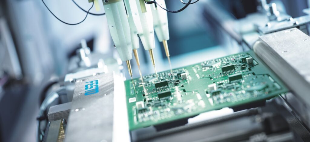
Printed Circuit Boards (PCBs) are the backbone of almost every electronic device we use today. From smartphones and laptops to medical equipment and automotive systems, PCBs make modern technology possible. Understanding PCB manufacturing and assembly is essential for engineers, businesses, and even hobbyists who want to design and bring electronic products to life. This guide covers everything you need to know about the process, from design to finished product.
What Is PCB Manufacturing and Assembly?
PCB manufacturing involves creating the physical board that connects and supports electronic components. This process includes designing the layout, etching copper traces, drilling holes, and layering materials to form the final board.
PCB assembly (PCBA) is the next step. It refers to the process of mounting and soldering components such as resistors, capacitors, and integrated circuits onto the manufactured PCB. Together, these processes transform raw boards into functional electronic circuits.
The Importance of PCBs in Modern Technology
PCBs are more than just circuit carriers—they define the performance, reliability, and efficiency of a device. Without them, electronics would be bulky, inefficient, and prone to errors. Key benefits include
- Compact design: Multiple layers allow complex circuits to fit in small devices.
- Reliable connections: Copper traces provide consistent electricalpathways.
- Cost efficiency: Mass production reduces costs for manufacturers.
- Scalability: From prototypes to millions of units, PCBs support mass production needs.
The PCB Manufacturing Process
Creating a PCB requires precision, advanced machinery, and multiple steps to ensure quality and functionality.
1. PCB Design
The process starts with design using software like Altium Designer, Eagle, or KiCad. Engineers create schematics and define the layout, including copper traces, vias, and component placement. The design is converted into Gerber files, the industry standard format used for manufacturing.
2. Substrate Preparation
The base of a PCB is usually fiberglass (FR4) or other insulating material. A thin layer of copper is laminated onto this substrate, forming the foundation for circuit paths.
3. Imaging and Etching
The circuit pattern from the design files is transferred onto the copper layer using photoresist. Unwanted copper is etched away with chemicals, leaving only the required conductive pathways.
4. Drilling
Holes for through-hole components and vias are drilled with precision machines. These holes are later plated with copper to ensure electrical connectivity between layers.
5. Plating and Layer Alignment
For multilayer boards, copper plating is applied to drilled holes and board surfaces. Layers are carefully aligned and pressed together under heat and pressure to create a single unit.
6. Solder Mask and Silkscreen
A solder mask is applied to insulate copper traces and prevent solder bridges during assembly. The silkscreen layer adds component identifiers, logos, and other markings for reference.
7. Surface Finishing
The exposed copper pads are coated with finishes such as HASL (Hot Air Solder Leveling), ENIG (Electroless Nickel Immersion Gold), or OSP (Organic Solderability Preservative) to enhance solderability and protect against oxidation.
8. Testing
Before leaving the factory, PCBs undergo electrical testing such as Flying Probe or In-Circuit Testing (ICT) to verify continuity and detect shorts or open circuits.
PCB Assembly Process
Once the bare board is manufactured, it moves to the assembly stage where components are added.
1. Solder Paste Application
For surface-mount technology (SMT), solder paste (a mix of tiny solder balls and flux) is applied to the pads using a stencil printer.
2. Component Placement
Pick-and-place machines automatically position tiny components onto the board with extreme accuracy. For complex boards, hundreds or even thousands of parts may be placed in seconds.
3. Reflow Soldering
The board passes through a reflow oven, where controlled heat melts the solder paste and permanently secures components.
4. Through-Hole Component Soldering
Larger components that require stronger mechanical support are mounted through drilled holes and soldered either manually or using wave soldering machines.
5. Inspection and Testing
Automated Optical Inspection (AOI) systems, X-ray inspection, and functional tests ensure that all parts are placed correctly and solder joints are strong.
Types of PCBs
Not all PCBs are the same. Depending on the application, different types are manufactured:
- Single-layer PCB: Basic design with one copper layer, ideal for simple electronics.
- Double-layer PCB: Two copper layers, offering more routing flexibility.
- Multilayer PCB: Multiple stacked layers, common in smartphones, computers, and medical devices.
- Rigid PCB: Solid fiberglass base for durability.
- Flexible PCB: Bendable polyimide base for compact devices.
- Rigid-Flex PCB: Combination of rigid and flexible sections, used in aerospace and medical equipment.
Challenges in PCB Manufacturing and Assembly
Despite technological advancements, manufacturers face several challenges:
- Miniaturization: Smaller devices require finer traces and micro-vias, increasing complexity.
- High-density designs: Smartphones and IoT devices need multilayer boards with advanced routing.
- Material selection: Choosing the right substrate for high-frequency or high-temperature applications is critical.
- Quality control: Even a small defect can cause device failure.
- Cost vs. performance: Balancing budget with quality requirements is a constant challenge.
Choosing the Right PCB Manufacturer
Selecting a reliable PCB manufacturer can make or break your project. Key factors to consider include:
- Experience and certifications: Look for ISO, UL, or IPC certifications.
- Technology capability: Ensure they can handle multilayer boards, HDI (High Density Interconnect), and fine pitch designs if required.
- Prototyping speed: Quick-turn services help speed up development cycles
- Testing and quality assurance: A strong testing protocol ensures reliability.
- Support and communication: Clear communication reduces errors and delays.
Future of PCB Manufacturing
The PCB industry continues to evolve with technology trends. Some future directions include:
- Miniaturization and 3D PCBs: Smaller, denser designs with advanced stacking methods.
- Eco-friendly materials: Push toward recyclable substrates and lead-free finishes.
- Integration with AI and IoT: PCBs designed for smart, connected devices.
- Advanced substrates: High-frequency boards for 5G, radar, and aerospace applications.
- Additive manufacturing: 3D printing of PCBs is an emerging technology that may revolutionize prototyping.
Conclusion
PCB manufacturing and assembly form the foundation of the electronics industry. From designing schematics to final testing, each step requires precision and expertise to create reliable products. As devices become smaller, faster, and more complex, PCB technology continues to advance. Whether you are an engineer, entrepreneur, or hobbyist, understanding the process gives you the knowledge to make informed decisions and bring innovative ideas to reality.